Note
Go to the end to download the full example code.
Lumped ports: investigations#
A PortLumped terminates a line in a single
chain of grid edges — cheap, DC-capable, and available where a
waveguide port window does not fit. The price is that it is not an
exact line termination: a residual self-reflection and a phase error
remain, and both depend on the grid at the gap, on the gap geometry
and position, and on the port impedance. Rules of thumb exist, but
none of them tells you how good your termination is on your mesh,
or up to which frequency you can trust it.
This page is the long answer: it builds the measurement setup once, then walks the three classic printed-line types — coaxial line, microstrip, coplanar waveguide — and shows, sweep by sweep, which design choice moves which error. Every number is a property of the example grids, not a constant of the method. For day-to-day work there is one tuning page per line type right after this one — a compact download-and-edit tool that reduces to: fill in your dimensions, run, read the scoreboard.
The measurement principle#
Two short runs per candidate termination:
A waveguide port — reflection-free by construction, with a floor far below anything a lumped element reaches — launches the exact line mode down a short uniform line onto the lumped port under test.
|S11|at the waveguide port is the termination’s self-reflection.A reference run of the same line with waveguide ports at both ends provides the phase ruler: its transmission phase is the exact propagation of this grid over the reference length, so the difference to the lumped run is the termination’s phase error — no textbook dispersion formula involved, which is what lets the same recipe serve dispersive lines unchanged.
One subtlety before reading any phase number: the sign of a solved
mode profile is a convention, so the relative polarity between a
lumped port and the waveguide mode is arbitrary by ±180°. A perfect
termination therefore shows a phase error of 0° or ±180° at low
frequency, depending on which way round its start/end points
happen to be. The helper below removes that convention by
referencing the error to the nearest multiple of 180° at the low end
of the band — what remains is the physical, frequency-dependent part.
import matplotlib.pyplot as plt
import numpy as np

import magnelio as mio
from magnelio import geo, ports

F_MAX = 15e9


def phase_error(result, ref, f):
    """Phase error against the reference run, polarity-normalised."""
    err = result.phase("dut", "wg") - ref.phase("far", "wg")
    lo = int(np.argmax(f >= F_MAX / 15.0))
    return err - 180.0 * np.round(err[lo] / 180.0)


def scoreboard(result, ref, label):
    f = np.asarray(result.f_axis)
    band = f <= F_MAX
    s11_db = result.db("wg", "wg")
    good = s11_db[band] < -20.0
    f_edge = f[band][np.argmin(good)] if not good.all() else f[band][-1]
    err = phase_error(result, ref, f)
    print(f"--- {label} ---")
    print(f"worst |S11| in band : {s11_db[band].max():6.1f} dB")
    print(f"|S11| < -20 dB up to: {f_edge / 1e9:6.2f} GHz")
    print(f"max |phase error|   : {np.abs(err[band]).max():6.2f} deg")
Coaxial line#
The coax termination is the classic: the inner conductor stops a gap short of a shorted end plate, and the lumped port bridges the gap on the axis. Three knobs: the gap length, the gap position relative to the reference plane, and the port impedance.
The test grid pins max_cell_size = min_cell_size: the feed is
uniform, so the reference run and the candidate runs see the same
line per unit length, and the cross-section cell size — the one
quantity you should copy from your production mesh — is the only
resolution parameter.
r_i = 0.405e-3  # inner conductor radius [m]
r_o = 1.475e-3  # shield (dielectric outer) radius [m]
eps_coax = 2.25  # solid polyethylene
cell = 0.5 * r_i  # production cross-section cell size [m]
L_coax = 5.0 * r_o  # waveguide port to reference plane [m]


def _coax_model(length, pin_length):
    model = mio.GeometryModel(background="pec")
    dielectric = geo.Cylinder(
        origin=(0.0, 0.0, 0.0),
        radius=r_o,
        height=length,
        axis="z",
        material=mio.Material.from_isotropic(name="polyethylene", epsilon=eps_coax),
    )
    inner = geo.Cylinder(
        origin=(0.0, 0.0, 0.0), radius=r_i, height=pin_length, axis="z", material="pec"
    )
    model.add(geo.Difference(dielectric, inner))
    model.add(inner)
    model.add_port(ports.PortWaveguide(name="wg", plane="zmin"))
    return model


def _coax_mesh(model):
    return mio.Mesh.from_geometry(
        model,
        mio.MeshControl(min_cell_size=cell, max_cell_size=cell),
        f_max=F_MAX,
    )


def reference_coax():
    model = _coax_model(L_coax, pin_length=L_coax)
    model.add_port(ports.PortWaveguide(name="far", plane="zmax"))
    return mio.AnalysisScatteringTD(mesh=_coax_mesh(model), verbose=False).run(excited=[("wg", 0)])


def measure_coax(gap, gap_position, z0=None):
    z_pin = L_coax + gap_position
    z_end = z_pin + gap
    model = _coax_model(z_end, pin_length=z_pin)
    mesh = _coax_mesh(model)
    z_line = mio.AnalysisScatteringTD(mesh=mesh, verbose=False).solve_ports()["wg"].z_line_num
    model.add_port(
        ports.PortLumped(
            name="dut",
            start=(0.0, 0.0, z_end),
            end=(0.0, 0.0, z_pin),
            Z0=float(z0 if z0 is not None else z_line),
        )
    )
    result = mio.AnalysisScatteringTD(mesh=mesh, ports=list(model.ports), verbose=False).run(
        excited=[("wg", 0)]
    )
    return result, z_line


gap0 = 0.4 * (r_o - r_i)
ref_coax = reference_coax()
f_c = np.asarray(ref_coax.f_axis)
band_c = f_c <= F_MAX

coax, z_coax = measure_coax(gap0, 0.0)
print(f"coax line impedance on this grid: {z_coax:.2f} Ohm")
scoreboard(coax, ref_coax, "coax, naive start values")
  mesh | feature planes
  mesh | grid lines
  mesh | materials
  mesh | conformal cells
  mesh | PEC masks
  mesh | 14 x 14 x 36 cells
  mesh | feature planes
  mesh | grid lines
  mesh | materials
  mesh | conformal cells
  mesh | PEC masks
  mesh | 14 x 14 x 38 cells
coax line impedance on this grid: 47.31 Ohm
--- coax, naive start values ---
worst |S11| in band :  -19.5 dB
|S11| < -20 dB up to:  14.18 GHz
max |phase error|   :  28.97 deg
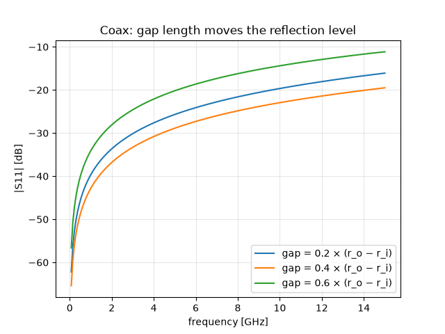
Gap length moves the broadband reflection level — the gap is a small series capacitor in front of the resistive port edge, and its reactance is what reflects at the top of the band.
fig, ax = plt.subplots()
for factor in (0.2, 0.4, 0.6):
    res_g, _ = measure_coax(factor * (r_o - r_i), 0.0)
    ax.plot(
        f_c[band_c] / 1e9,
        res_g.db("wg", "wg")[band_c],
        label=f"gap = {factor:.1f} × (r_o − r_i)",
    )
ax.set_xlabel("frequency [GHz]")
ax.set_ylabel("|S11| [dB]")
ax.set_title("Coax: gap length moves the reflection level")
ax.grid(True, alpha=0.3)
ax.legend()
  mesh | feature planes
  mesh | grid lines
  mesh | materials
  mesh | conformal cells
  mesh | PEC masks
  mesh | 14 x 14 x 37 cells
  mesh | feature planes
  mesh | grid lines
  mesh | materials
  mesh | conformal cells
  mesh | PEC masks
  mesh | 14 x 14 x 38 cells
  mesh | feature planes
  mesh | grid lines
  mesh | materials
  mesh | conformal cells
  mesh | PEC masks
  mesh | 14 x 14 x 39 cells

<matplotlib.legend.Legend object at 0x7f2c2ffaf890>
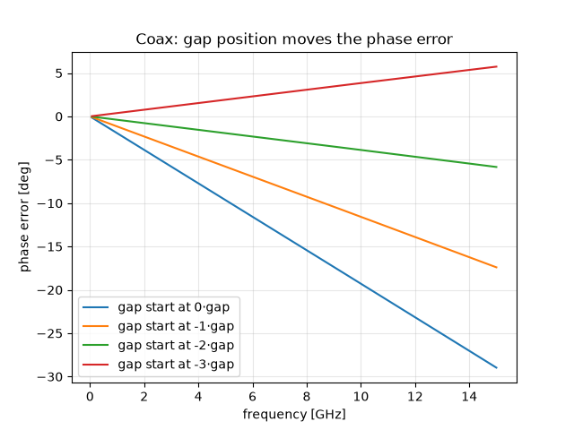
Gap position moves the phase error. The termination does not act at the end plate — the fields detour around the pin end — so the gap has to sit off the reference plane to compensate. Each candidate is its own geometry and its own run, exactly as in the target simulation, where this one position is the compromise you commit to. On this TEM line the best position works across the whole band; hold that thought for the microstrip section.
fig, ax = plt.subplots()
for k in (0.0, -1.0, -2.0, -3.0):
    res_k, _ = measure_coax(gap0, k * gap0)
    err_k = phase_error(res_k, ref_coax, f_c)
    ax.plot(f_c[band_c] / 1e9, err_k[band_c], label=f"gap start at {k:.0f}·gap")
    worst = np.abs(err_k[band_c]).max()
    print(f"coax, gap start at {k:.0f}·gap: max |phase error| {worst:6.2f} deg")
ax.set_xlabel("frequency [GHz]")
ax.set_ylabel("phase error [deg]")
ax.set_title("Coax: gap position moves the phase error")
ax.grid(True, alpha=0.3)
ax.legend()
  mesh | feature planes
  mesh | grid lines
  mesh | materials
  mesh | conformal cells
  mesh | PEC masks
  mesh | 14 x 14 x 38 cells
coax, gap start at 0·gap: max |phase error|  28.97 deg
  mesh | feature planes
  mesh | grid lines
  mesh | materials
  mesh | conformal cells
  mesh | PEC masks
  mesh | 14 x 14 x 36 cells
coax, gap start at -1·gap: max |phase error|  17.40 deg
  mesh | feature planes
  mesh | grid lines
  mesh | materials
  mesh | conformal cells
  mesh | PEC masks
  mesh | 14 x 14 x 34 cells
coax, gap start at -2·gap: max |phase error|   5.83 deg
  mesh | feature planes
  mesh | grid lines
  mesh | materials
  mesh | conformal cells
  mesh | PEC masks
  mesh | 14 x 14 x 32 cells
coax, gap start at -3·gap: max |phase error|   5.74 deg

<matplotlib.legend.Legend object at 0x7f2c362efd10>
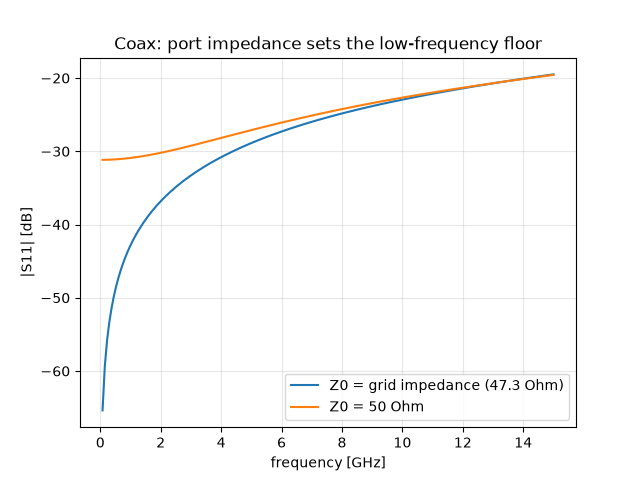
Port impedance sets the low-frequency floor: the constant mismatch \((Z - Z_0)/(Z + Z_0)\) is what remains when all reactive effects have died out. The line impedance of the grid — what the waveguide-port solver reports — differs from the closed-form value on a coarse cross-section, and using it instead of the catalogue number removes the deterministic part of the mismatch.
res_50, _ = measure_coax(gap0, 0.0, z0=50.0)
fig, ax = plt.subplots()
ax.plot(
    f_c[band_c] / 1e9,
    coax.db("wg", "wg")[band_c],
    label=f"Z0 = grid impedance ({z_coax:.1f} Ohm)",
)
ax.plot(f_c[band_c] / 1e9, res_50.db("wg", "wg")[band_c], label="Z0 = 50 Ohm")
ax.set_xlabel("frequency [GHz]")
ax.set_ylabel("|S11| [dB]")
ax.set_title("Coax: port impedance sets the low-frequency floor")
ax.grid(True, alpha=0.3)
ax.legend()
  mesh | feature planes
  mesh | grid lines
  mesh | materials
  mesh | conformal cells
  mesh | PEC masks
  mesh | 14 x 14 x 38 cells

<matplotlib.legend.Legend object at 0x7f2be6097890>
Microstrip#
The standard microstrip termination is a vertical lumped port from the end of the trace straight down to the ground plane. There is no gap-length knob — the element length is the substrate height — so the knobs are the trace-end position and the impedance.
The cross-section is the shielded microstrip of the tutorials (FR4, 0.8 mm, 1.2 mm trace for ≈50 Ω); behind the trace end, substrate and air continue for a short tail before the shield’s back wall, as they would in a real layout.
h_sub = 0.8e-3
w_strip = 1.2e-3
t_met = 0.2e-3
eps_pcb = 4.3
W_box, H_box = 8.0e-3, 5.0e-3
L_ms = 5.0 * w_strip
tail = 2.5 * h_sub


def _ms_model(length, strip_len):
    fr4 = mio.Material.from_isotropic(name="FR4", epsilon=eps_pcb)
    model = mio.GeometryModel(background="pec")
    model.add(geo.Brick(origin=(-W_box / 2, 0.0, 0.0), size=(W_box, h_sub, length), material=fr4))
    air = geo.Brick(
        origin=(-W_box / 2, h_sub, 0.0), size=(W_box, H_box - h_sub, length), material="air"
    )
    strip = geo.Brick(
        origin=(-w_strip / 2, h_sub, 0.0), size=(w_strip, t_met, strip_len), material="pec"
    )
    model.add(geo.Difference(air, strip))
    model.add(strip)
    model.add_port(ports.PortWaveguide(name="wg", plane="zmin", n_modes=1))
    return model


def _pcb_mesh(model):
    return mio.Mesh.from_geometry(
        model,
        mio.MeshControl(min_nodes_per_wavelength=25),
        f_max=F_MAX,
    )


def reference_ms():
    model = _ms_model(L_ms, strip_len=L_ms)
    model.add_port(ports.PortWaveguide(name="far", plane="zmax", n_modes=1))
    return mio.AnalysisScatteringTD(mesh=_pcb_mesh(model), verbose=False).run(excited=[("wg", 0)])


def measure_ms(end_position, z0=None):
    z_pin = L_ms + end_position
    model = _ms_model(z_pin + tail, strip_len=z_pin)
    mesh = _pcb_mesh(model)
    z_line = mio.AnalysisScatteringTD(mesh=mesh, verbose=False).solve_ports()["wg"].modes[0].z_line
    model.add_port(
        ports.PortLumped(
            name="dut",
            start=(0.0, h_sub, z_pin),
            end=(0.0, 0.0, z_pin),
            Z0=float(z0 if z0 is not None else z_line),
        )
    )
    result = mio.AnalysisScatteringTD(mesh=mesh, ports=list(model.ports), verbose=False).run(
        excited=[("wg", 0)]
    )
    return result, z_line


ref_ms = reference_ms()
f_m = np.asarray(ref_ms.f_axis)
band_m = f_m <= F_MAX

ms, z_ms = measure_ms(0.0)
print(f"microstrip line impedance on this grid: {z_ms:.2f} Ohm")
scoreboard(ms, ref_ms, "microstrip, trace end at the reference plane")
  mesh | feature planes
  mesh | grid lines
  mesh | materials
  mesh | conformal cells
  mesh | PEC masks
  mesh | 24 x 23 x 16 cells
  mesh | feature planes
  mesh | grid lines
  mesh | materials
  mesh | conformal cells
  mesh | PEC masks
  mesh | 24 x 23 x 22 cells
microstrip line impedance on this grid: 50.23 Ohm
--- microstrip, trace end at the reference plane ---
worst |S11| in band :  -14.4 dB
|S11| < -20 dB up to:   5.97 GHz
max |phase error|   :  23.73 deg
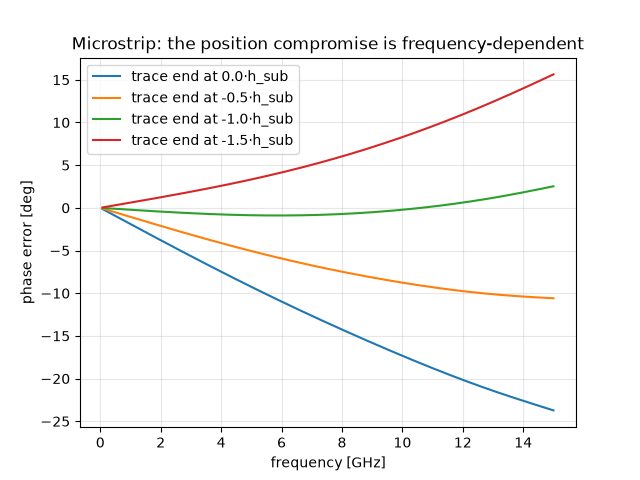
The position sweep again — with one difference to the coax. A microstrip is dispersive: ε_eff rises with frequency, so the electrical length the end effect adds is not a fixed fraction of a wavelength. The curves therefore tilt rather than shift, and the chosen position is a genuine band compromise: pick it for the part of the band that matters most in your application.
fig, ax = plt.subplots()
for k in (0.0, -0.5, -1.0, -1.5):
    res_k, _ = measure_ms(k * h_sub)
    err_k = phase_error(res_k, ref_ms, f_m)
    ax.plot(f_m[band_m] / 1e9, err_k[band_m], label=f"trace end at {k:.1f}·h_sub")
    worst = np.abs(err_k[band_m]).max()
    print(f"microstrip, trace end at {k:.1f}·h_sub: max |phase error| {worst:6.2f} deg")
ax.set_xlabel("frequency [GHz]")
ax.set_ylabel("phase error [deg]")
ax.set_title("Microstrip: the position compromise is frequency-dependent")
ax.grid(True, alpha=0.3)
ax.legend()
  mesh | feature planes
  mesh | grid lines
  mesh | materials
  mesh | conformal cells
  mesh | PEC masks
  mesh | 24 x 23 x 22 cells
microstrip, trace end at 0.0·h_sub: max |phase error|  23.73 deg
  mesh | feature planes
  mesh | grid lines
  mesh | materials
  mesh | conformal cells
  mesh | PEC masks
  mesh | 24 x 23 x 21 cells
microstrip, trace end at -0.5·h_sub: max |phase error|  10.59 deg
  mesh | feature planes
  mesh | grid lines
  mesh | materials
  mesh | conformal cells
  mesh | PEC masks
  mesh | 24 x 23 x 20 cells
microstrip, trace end at -1.0·h_sub: max |phase error|   2.53 deg
  mesh | feature planes
  mesh | grid lines
  mesh | materials
  mesh | conformal cells
  mesh | PEC masks
  mesh | 24 x 23 x 19 cells
microstrip, trace end at -1.5·h_sub: max |phase error|  15.63 deg

<matplotlib.legend.Legend object at 0x7f2be60e13d0>
Coplanar waveguide#
The CPW termination is, once the model exploits the pair’s
symmetry, the coax picture again: the centre strip stops an end
gap short of the ground metallisation behind it — one boolean cut
shapes strip, slots, end gap and closing ground plate in a single
stroke — and the lumped port bridges the gap longitudinally, on the
symmetry plane. Declaring that plane as a magnetic wall
(xmin="SymmetryPMC") halves the model and keeps the port
centred on the even mode; without the symmetry plane a centred
single-edge port would not exist and both slots would have to be
loaded separately. The structure is open above (a PMC lid, not a
metal cover) and the substrate floats on air below — a plain,
ungrounded CPW.
The knobs are the coax knobs: end-gap width, end-gap position, port impedance.
w_cpw = 0.7e-3  # centre strip width
s_cpw = 0.05e-3  # slot width
h_cpw = 0.508e-3  # substrate height
t_cpw = 17e-6  # metallisation thickness
eps_cpw = 3.38  # Rogers 4003
a_air = 10 * s_cpw  # air above the metallisation
b_air = 5 * s_cpw  # air below the substrate
L_cpw = 5.0 * w_cpw
p_gnd = 3.0 * (w_cpw / 2 + s_cpw)
X_cpw = w_cpw / 2 + s_cpw + p_gnd


def _cpw_model(strip_end=None, gap=None):
    z_lo = -L_cpw
    z_hi = (0.0 if strip_end is None else strip_end + gap) + p_gnd
    diel = mio.Material.from_isotropic(epsilon=eps_cpw, name="rogers4003")
    lift = geo.Brick.from_ranges(
        x1=-X_cpw, x2=X_cpw, y1=-h_cpw - b_air, y2=-h_cpw, z1=z_lo, z2=z_hi, material="air"
    )
    subst = geo.Brick.from_ranges(
        x1=-X_cpw, x2=X_cpw, y1=-h_cpw, y2=0, z1=z_lo, z2=z_hi, material=diel
    )
    air = geo.Brick.from_ranges(
        x1=-X_cpw, x2=X_cpw, y1=0, y2=a_air, z1=z_lo, z2=z_hi, material="air"
    )
    metal = geo.Brick.from_ranges(
        x1=-X_cpw, x2=X_cpw, y1=0, y2=t_cpw, z1=z_lo, z2=z_hi, material="pec"
    )
    cut_z2 = z_hi + 1.0 if strip_end is None else strip_end + gap
    metal -= geo.Brick.from_ranges(
        x1=-w_cpw / 2 - s_cpw, x2=w_cpw / 2 + s_cpw, y1=-1, y2=1, z1=-1, z2=cut_z2
    )
    strip_z2 = z_hi if strip_end is None else strip_end
    metal += geo.Brick.from_ranges(
        x1=-w_cpw / 2, x2=w_cpw / 2, y1=0, y2=t_cpw, z1=z_lo, z2=strip_z2, material="pec"
    )
    model = mio.GeometryModel(
        background="air",
        boundary_conditions={"xmin": "SymmetryPMC", "ymax": "PMC"},
    )
    model.add([lift, subst, metal, air - metal])
    model.add_port(
        ports.PortWaveguide(
            name="wg", plane="zmin", corners=((-1, -1, None), (1, 1, None)), n_modes=1
        )
    )
    return model


def _cpw_mesh(model):
    return mio.Mesh.from_geometry(model, mio.MeshControl(min_cell_size=s_cpw / 4), f_max=F_MAX)


def reference_cpw():
    model = _cpw_model()
    model.add_port(
        ports.PortWaveguide(
            name="far", plane="zmax", corners=((-1, -1, None), (1, 1, None)), n_modes=1
        )
    )
    return mio.AnalysisScatteringTD(mesh=_cpw_mesh(model), verbose=False).run(excited=[("wg", 0)])


def measure_cpw(gap, gap_position, z0=None):
    model = _cpw_model(strip_end=gap_position, gap=gap)
    mesh = _cpw_mesh(model)
    z_line = mio.AnalysisScatteringTD(mesh=mesh, verbose=False).solve_ports()["wg"].z_line_num
    model.add_port(
        ports.PortLumped(
            name="dut",
            start=(0.0, 0.0, gap_position),
            end=(0.0, 0.0, gap_position + gap),
            Z0=float(z0 if z0 is not None else z_line),
        )
    )
    mesh = _cpw_mesh(model)  # rebuild: the mesh carries the port
    result = mio.AnalysisScatteringTD(mesh=mesh, verbose=False).run(excited=[("wg", 0)])
    return result, z_line


ref_cpw = reference_cpw()
f_w = np.asarray(ref_cpw.f_axis)
band_w = f_w <= F_MAX

cpw, z_cpw = measure_cpw(s_cpw, 0.0)
print(f"CPW line impedance on this grid: {z_cpw:.2f} Ohm")
scoreboard(cpw, ref_cpw, "CPW, naive start values")
  mesh | feature planes
  mesh | grid lines
  mesh | materials
  mesh | conformal cells
  mesh | PEC masks
  mesh | 23 x 31 x 9 cells
  mesh | feature planes
  mesh | grid lines
  mesh | materials
  mesh | conformal cells
  mesh | PEC masks
  mesh | 23 x 31 x 33 cells
  mesh | feature planes
  mesh | grid lines
  mesh | materials
  mesh | conformal cells
  mesh | PEC masks
  mesh | 23 x 31 x 33 cells
CPW line impedance on this grid: 42.22 Ohm
--- CPW, naive start values ---
worst |S11| in band :  -26.6 dB
|S11| < -20 dB up to:  15.00 GHz
max |phase error|   :  21.35 deg
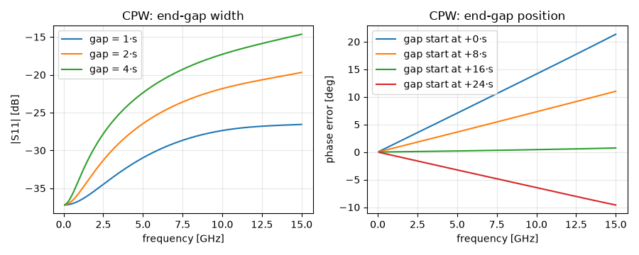
The two geometric knobs, swept. The gap-width sweep mirrors the coax; the position sweep runs toward positive offsets — the current returning through the ground plate behind the gap lengthens the effective line, so the gap wants to sit noticeably beyond the reference plane on this structure.
fig, (ax1, ax2) = plt.subplots(1, 2, figsize=(9.0, 3.6))
for factor in (1.0, 2.0, 4.0):
    res_g, _ = measure_cpw(factor * s_cpw, 0.0)
    ax1.plot(
        f_w[band_w] / 1e9,
        res_g.db("wg", "wg")[band_w],
        label=f"gap = {factor:.0f}·s",
    )
ax1.set_xlabel("frequency [GHz]")
ax1.set_ylabel("|S11| [dB]")
ax1.set_title("CPW: end-gap width")
ax1.grid(True, alpha=0.3)
ax1.legend()

for k in (0.0, 8.0, 16.0, 24.0):
    res_k, _ = measure_cpw(s_cpw, k * s_cpw)
    err_k = phase_error(res_k, ref_cpw, f_w)
    ax2.plot(f_w[band_w] / 1e9, err_k[band_w], label=f"gap start at +{k:.0f}·s")
    worst = np.abs(err_k[band_w]).max()
    print(f"CPW, gap start at +{k:.0f}·s: max |phase error| {worst:6.2f} deg")
ax2.set_xlabel("frequency [GHz]")
ax2.set_ylabel("phase error [deg]")
ax2.set_title("CPW: end-gap position")
ax2.grid(True, alpha=0.3)
ax2.legend()
fig.tight_layout()
  mesh | feature planes
  mesh | grid lines
  mesh | materials
  mesh | conformal cells
  mesh | PEC masks
  mesh | 23 x 31 x 33 cells
  mesh | feature planes
  mesh | grid lines
  mesh | materials
  mesh | conformal cells
  mesh | PEC masks
  mesh | 23 x 31 x 33 cells
  mesh | feature planes
  mesh | grid lines
  mesh | materials
  mesh | conformal cells
  mesh | PEC masks
  mesh | 23 x 31 x 31 cells
  mesh | feature planes
  mesh | grid lines
  mesh | materials
  mesh | conformal cells
  mesh | PEC masks
  mesh | 23 x 31 x 31 cells
  mesh | feature planes
  mesh | grid lines
  mesh | materials
  mesh | conformal cells
  mesh | PEC masks
  mesh | 23 x 31 x 25 cells
  mesh | feature planes
  mesh | grid lines
  mesh | materials
  mesh | conformal cells
  mesh | PEC masks
  mesh | 23 x 31 x 25 cells
  mesh | feature planes
  mesh | grid lines
  mesh | materials
  mesh | conformal cells
  mesh | PEC masks
  mesh | 23 x 31 x 33 cells
  mesh | feature planes
  mesh | grid lines
  mesh | materials
  mesh | conformal cells
  mesh | PEC masks
  mesh | 23 x 31 x 33 cells
CPW, gap start at +0·s: max |phase error|  21.35 deg
  mesh | feature planes
  mesh | grid lines
  mesh | materials
  mesh | conformal cells
  mesh | PEC masks
  mesh | 23 x 31 x 34 cells
  mesh | feature planes
  mesh | grid lines
  mesh | materials
  mesh | conformal cells
  mesh | PEC masks
  mesh | 23 x 31 x 34 cells
CPW, gap start at +8·s: max |phase error|  11.02 deg
  mesh | feature planes
  mesh | grid lines
  mesh | materials
  mesh | conformal cells
  mesh | PEC masks
  mesh | 23 x 31 x 35 cells
  mesh | feature planes
  mesh | grid lines
  mesh | materials
  mesh | conformal cells
  mesh | PEC masks
  mesh | 23 x 31 x 35 cells
CPW, gap start at +16·s: max |phase error|   0.74 deg
  mesh | feature planes
  mesh | grid lines
  mesh | materials
  mesh | conformal cells
  mesh | PEC masks
  mesh | 23 x 31 x 35 cells
  mesh | feature planes
  mesh | grid lines
  mesh | materials
  mesh | conformal cells
  mesh | PEC masks
  mesh | 23 x 31 x 35 cells
CPW, gap start at +24·s: max |phase error|   9.60 deg
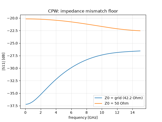
And the impedance floor, as before: the grid’s line impedance sits well away from a nominal 50 Ω here, so terminating with the catalogue value leaves a visible broadband pedestal.
cpw_50, _ = measure_cpw(s_cpw, 0.0, z0=50.0)
fig, ax = plt.subplots()
ax.plot(f_w[band_w] / 1e9, cpw.db("wg", "wg")[band_w], label=f"Z0 = grid ({z_cpw:.1f} Ohm)")
ax.plot(f_w[band_w] / 1e9, cpw_50.db("wg", "wg")[band_w], label="Z0 = 50 Ohm")
ax.set_xlabel("frequency [GHz]")
ax.set_ylabel("|S11| [dB]")
ax.set_title("CPW: impedance mismatch floor")
ax.grid(True, alpha=0.3)
ax.legend()
  mesh | feature planes
  mesh | grid lines
  mesh | materials
  mesh | conformal cells
  mesh | PEC masks
  mesh | 23 x 31 x 33 cells
  mesh | feature planes
  mesh | grid lines
  mesh | materials
  mesh | conformal cells
  mesh | PEC masks
  mesh | 23 x 31 x 33 cells

<matplotlib.legend.Legend object at 0x7f2c0251f690>
What carries over#
Across all three line types the same three-part picture:
the end-gap geometry (gap width; for microstrip the fixed substrate height) sets the broadband reflection level;
the position of the termination relative to the reference plane sets the phase error — exactly compensable on TEM lines, a band compromise on dispersive ones;
the port impedance sets the low-frequency floor, and the right value is the line impedance of the grid, read from the waveguide-port solve, not the catalogue number.
Symmetry is the CPW’s friend: the magnetic wall through the strip centre is what lets a single edge chain terminate the even mode the way the coax pin gap does. And keep the test fixture itself above suspicion — its shield (if any) single-mode over the band, its resolution the resolution of the production model.
None of the optima transfer between grids. The per-line tuning pages package this measurement as a compact tool: fill in the given quantities of your production model, run, and read the scoreboard.
for res, refr, lbl in ((coax, ref_coax, "coax"), (ms, ref_ms, "microstrip"), (cpw, ref_cpw, "CPW")):
    scoreboard(res, refr, f"{lbl}, naive start values")
--- coax, naive start values ---
worst |S11| in band :  -19.5 dB
|S11| < -20 dB up to:  14.18 GHz
max |phase error|   :  28.97 deg
--- microstrip, naive start values ---
worst |S11| in band :  -14.4 dB
|S11| < -20 dB up to:   5.97 GHz
max |phase error|   :  23.73 deg
--- CPW, naive start values ---
worst |S11| in band :  -26.6 dB
|S11| < -20 dB up to:  15.00 GHz
max |phase error|   :  21.35 deg
Total running time of the script: (1 minutes 2.475 seconds)