Note
Go to the end to download the full example code.
A coaxial line: solids, booleans, and a coax port#
The first tutorial needed no geometry at all — one air brick, and every conductor was a boundary face. This one builds a real three-dimensional structure: a short piece of RG-58 class coaxial cable, modelled from solid primitives and a boolean operation. Along the way it introduces the second way of declaring a port — by naming the analytical family of its cross-section — and the habit of reading a port report that carries both a numerical and a reference impedance.
The problem#
A coaxial line guides a TEM wave between an inner conductor of radius \(r_i\) and a shield of radius \(r_o\), filled with a dielectric of permittivity \(\varepsilon_r\). Its line impedance has a closed form,
which makes it the classic first “real” validation case. We use the dimensions of an RG-58 class cable — solid polyethylene, \(r_i = 0.405\) mm, \(r_o = 1.475\) mm, \(\varepsilon_r = 2.25\) — giving \(Z_0 \approx 51.7\) Ohm. The first higher-order coax mode (TE11) appears near 34 GHz; simulating up to 6 GHz keeps us safely in the single-mode TEM band, so the S-parameters stay plain S11 and S21.
import math

import matplotlib.pyplot as plt
import numpy as np

import magnelio as mio
from magnelio import geo, plots, ports
from magnelio.constants import *

r_i = 0.405e-3  # inner conductor radius [m]
r_o = 1.475e-3  # shield (dielectric outer) radius [m]
eps_r = 2.25  # solid polyethylene
L = 8e-3  # line length [m]
f_max = 6e9  # upper band edge [Hz]

z_formula = ETA0 / (2 * math.pi * math.sqrt(eps_r)) * math.log(r_o / r_i)
print(f"target impedance: {z_formula:.3f} Ohm")
target impedance: 51.665 Ohm
Building the geometry#
Two solids and one boolean are enough:
the dielectric is a
Cylinderof radiusr_owith the inner conductor’sCylindercarved out of it —Differenceproduces the annulus;the inner conductor is the small cylinder itself, added as PEC.
The shield is not drawn at all. The model’s background material —
what fills every cell no shape claims — is set to PEC, and the
domain boundary closes as PEC by default. Everything outside the
dielectric, including the box corners around the circle, is
therefore solid conductor: the shield comes for free, and its inner
surface is exactly the dielectric boundary at r_o.
polyethylene = mio.Material.from_isotropic(name="polyethylene", epsilon=eps_r)

dielectric = geo.Cylinder(
    origin=(0.0, 0.0, 0.0), radius=r_o, height=L, axis="z", material=polyethylene
)
inner = geo.Cylinder(origin=(0.0, 0.0, 0.0), radius=r_i, height=L, axis="z", material="pec")

model = mio.GeometryModel(background="pec")
model.add(geo.Difference(dielectric, inner))  # the dielectric annulus
model.add(inner)  # the inner conductor
GeometryModel(2 shapes, background=PEC)
Looking at the model in three dimensions#
model.show() shows the model in three dimensions. On this page
it is a picture; in a Jupyter notebook the same call opens a
rotatable, zoomable view with a cutting plane driven from its
toolbar — the fastest way to check that a boolean did what you
meant. Every tutorial can be downloaded as a notebook (the link at
the bottom of the page), so this is one call away at any point.
Here the model is opened along its axis to show the annulus around
the inner conductor.
model.show(cut=("y", 0.0))
The coax port#
In the first tutorial, PortWaveguide simply
said “solve whatever modes this cross-section has”. When the
cross-section belongs to a family with a closed-form solution, a
PortAnalytical says so explicitly. The
port still solves its mode on the actual grid — but the report will
carry the analytical value alongside, as a built-in cross-check.
model.add_port(
    ports.PortAnalytical(
        name="port1",
        plane="zmin",
        family="coax",
        inner_radius=r_i,
        outer_radius=r_o,
        epsilon_r=eps_r,
    )
)
model.add_port(
    ports.PortAnalytical(
        name="port2",
        plane="zmax",
        family="coax",
        inner_radius=r_i,
        outer_radius=r_o,
        epsilon_r=eps_r,
    )
)
GeometryModel(2 shapes, background=PEC)
Mesh#
At 6 GHz the wavelength is huge compared to the cable, so the mesh size is dictated entirely by the geometry: the grid has to resolve the annulus. A 0.12 mm cap gives about nine cells across the dielectric gap.
mesh = mio.Mesh.from_geometry(model, mio.MeshControl(max_cell_size=0.12e-3), f_max=f_max)
print(f"grid: {mesh.Nx} x {mesh.Ny} x {mesh.Nz} cells")
  mesh | feature planes
  mesh | grid lines
  mesh | materials
  mesh | conformal cells
  mesh | conformal cells | done (5.3 s)
  mesh | PEC masks
  mesh | 25 x 25 x 67 cells (5.4 s total)
grid: 25 x 25 x 67 cells
Which geometry put each grid line where it is? The mesh keeps that
record. Every plane lists the rule and the shape that asked for it:
here the tangent planes of the two cylinders (face) and the
bounding boxes that coincide with them (extent); domain end
marks the box. A plane you cannot explain from this list is a plane
worth questioning.
print(mesh.planes)
Grid planes — feature gap 0.117 µm; nodes x 26, y 26, z 68
x: 4 planes  (h_bulk 1.666 mm, h_fine 0.2025 mm)
  [0]  -1.475 mm   face #0 Difference(polyethylene); extent #0   domain end
  [1]  -0.405 mm   face #0 Difference(polyethylene) #1 Cylinder(PEC); extent #1
  [2]   0.405 mm   face #0 Difference(polyethylene) #1 Cylinder(PEC); extent #1
  [3]   1.475 mm   face #0 Difference(polyethylene); extent #0   domain end
y: 4 planes  (h_bulk 1.666 mm, h_fine 0.2025 mm)
  [0]  -1.475 mm   face #0 Difference(polyethylene); extent #0   domain end
  [1]  -0.405 mm   face #0 Difference(polyethylene) #1 Cylinder(PEC); extent #1
  [2]   0.405 mm   face #0 Difference(polyethylene) #1 Cylinder(PEC); extent #1
  [3]   1.475 mm   face #0 Difference(polyethylene); extent #0   domain end
z: 2 planes  (h_bulk 1.666 mm, h_fine 1.666 mm)
  [0]  0 mm   face #0 Difference(polyethylene) #1 Cylinder(PEC); edge #0 #1; extent #0 #1   domain end
  [1]  8 mm   face #0 Difference(polyethylene) #1 Cylinder(PEC); edge #0 #1; extent #0 #1   domain end
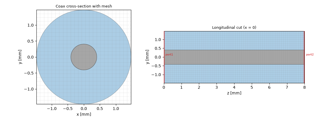
The 3D view shows the line opened along its axis, the grid cells on the cut coloured by material, and the two port windows on the domain faces.
model.show(mesh=mesh, cut=("y", 0.0))

# Two cuts: across the cable, and along it.  The longitudinal cut
# shows that the grid is uniform along the line — nothing varies in
# z, so nothing there needs resolving.
fig, axes = plt.subplots(1, 2, figsize=(11, 4.2))
plots.plot_cross_section(
    model, "z", L / 2, mesh=mesh, ax=axes[0], title="Coax cross-section with mesh"
)
plots.plot_cross_section(
    model, "x", 0.0, mesh=mesh, ax=axes[1], flip=True, title="Longitudinal cut (x = 0)"
)
fig.tight_layout()
The same section seen from the mesh’s side, three times. Every grid line is drawn in the style of the rule that placed it — material faces solid, the graded fill between them as hairlines — and the exact contour on top. What differs is the cell shading.
Left, the classification: the material whose volume contains each cell’s centre. A circle on a rectangular grid looks like a staircase here, and this picture is often mistaken for the accuracy of the discretisation. It is not — it is only the baseline the sub-cell treatment starts from.
Middle, the coverage: the exact area share of each cell that lies inside a conductor, as the sub-cell classifier measured it. The pin is a disc again and the outer wall a smooth ring. The edge layer adds what happens on the grid lines: edges held at conductor potential in dark grey, edges only partly inside the conductor in orange, and the short ones the solver lends to a longer neighbour marked with a cross.
Right, the permittivity the electric material matrix holds for the field component normal to the cut, on the dual cells around the nodes (0 = conductor). Edges running along a conductor surface are held at its potential, so the masked cells reach one node beyond the contour. For a TEM line this component carries no field; the picture matters for structures with a field along the cut normal.
fig, axes = plt.subplots(1, 3, figsize=(16, 4.8))
plots.plot_mesh_section(
    mesh,
    "z",
    L / 2,
    geometry=model,
    fill="material",
    ax=axes[0],
    legend=False,
    title="Cell classification",
)
plots.plot_mesh_section(
    mesh,
    "z",
    L / 2,
    geometry=model,
    fill="coverage",
    edges=True,
    ax=axes[1],
    title="Conductor coverage and edge treatment",
)
plots.plot_mesh_section(
    mesh,
    "z",
    L / 2,
    geometry=model,
    fill="conformal",
    ax=axes[2],
    legend=False,
    title="Permittivity seen by the normal component",
)
fig.tight_layout()
The middle picture is the one to keep in mind when reading the port report below: the conductor contours enter the material matrices with their exact area and length shares, not as the staircase on the left.
Numerical mode vs. analytical reference#
analysis = mio.AnalysisScatteringTD(mesh=mesh, verbose=False)

report = analysis.solve_ports()["port1"]
print(report)

z_num = report.z_line_num
z_ref = report.z_line_ref
print(f"z_line numerical : {z_num:7.2f} Ohm  ({100 * (z_num / z_ref - 1):+.1f} %)")
print(f"z_line reference : {z_ref:7.2f} Ohm")
Port 'port1' — 1 mode(s)
  z_line = 49.67 Ω (on this grid), 51.67 Ω (analytical reference, Δ -3.87 %)
  [0] TEM_lap00    TEM f_c = 0.0000 GHz  z_line = 49.67 Ω  ε_eff = 2.250  termination = dtbc (chain floor <= -320 dB)
z_line numerical :   49.67 Ohm  (-3.9 %)
z_line reference :   51.67 Ohm
The two impedances answer different questions. The reference is the closed-form value of the ideal circular line — the design target. The numerical value is the impedance of the staircased cross-section the grid actually represents; it differs by a few percent here and approaches the reference as the mesh is refined (not monotonically — the staircase reshapes at every resolution). The gap between the two is an honest measure of how well the mesh captures this cross-section.
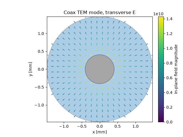
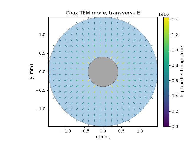
The transverse mode profile shows the expected radial TEM field, strongest at the inner conductor. Passing the geometry model overlays the port-plane cross-section — the grey disc is the inner conductor, the tinted annulus the dielectric:
Run and S-parameters#
result = analysis.run(excited=[("port1", 0)])

f = result.f_axis
s11_db = result.db("port1", "port1")
s21_db = result.db("port2", "port1")

fig, ax = plt.subplots()
ax.plot(f / 1e9, s11_db, label="|S11|")
ax.plot(f / 1e9, s21_db, label="|S21|")
ax.set_xlabel("frequency [GHz]")
ax.set_ylabel("magnitude [dB]")
ax.set_title("RG-58 class coax, 8 mm")
ax.grid(True)
ax.legend()

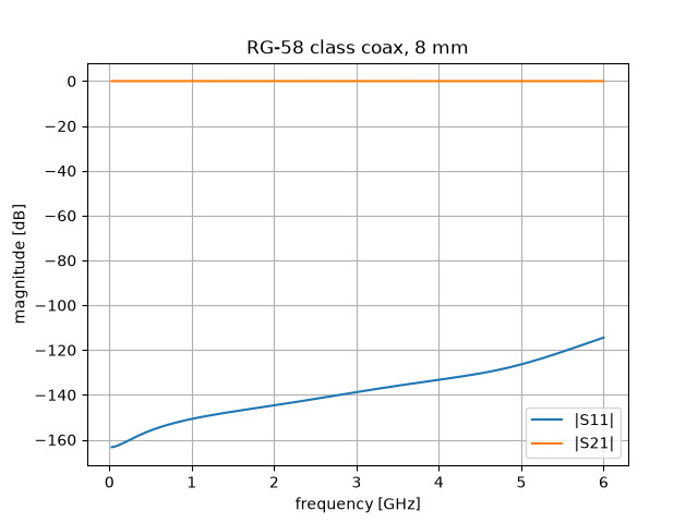
print(f"max |S11| in band: {s11_db.max():6.1f} dB")
max |S11| in band: -114.4 dB
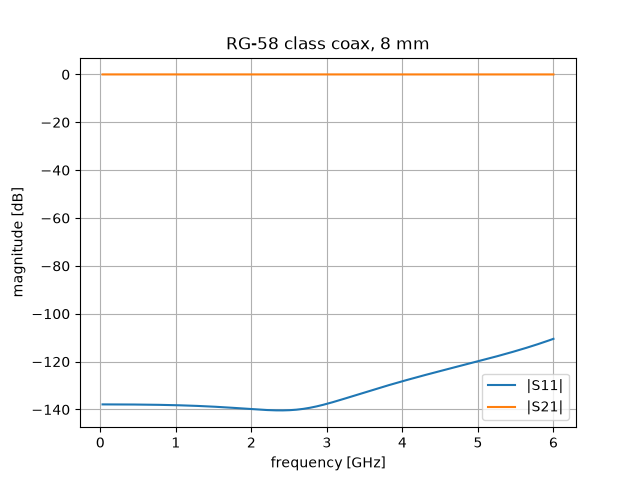
As for every uniform matched line, |S21| sits at 0 dB and
|S11| at the numerical floor — around -110 dB here. Note what that floor
means: the port’s discrete mode matches the discrete line so well
that essentially nothing reflects, even though the staircased
impedance differs from the ideal one by a few percent. Port
matching is between port and grid; the reference impedance is
between grid and reality.
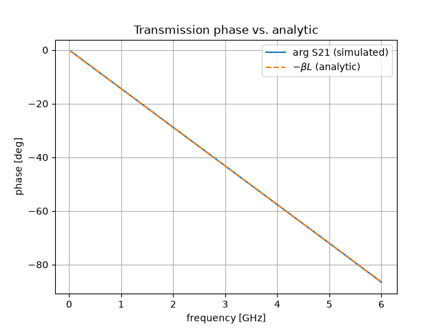
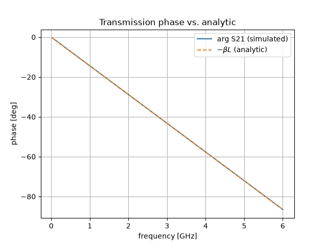
The transmission phase must follow the dielectric-loaded electrical length \(\beta L\) with \(\beta = 2 \pi f \sqrt{\varepsilon_r} / c_0\):
s21 = result.S("port2", "port1")
phase_sim = np.unwrap(np.angle(s21))
phase_ref = -2 * np.pi * f * math.sqrt(eps_r) / C0 * L

fig, ax = plt.subplots()
ax.plot(f / 1e9, np.degrees(phase_sim), label="arg S21 (simulated)")
ax.plot(f / 1e9, np.degrees(phase_ref), "--", label=r"$-\beta L$ (analytic)")
ax.set_xlabel("frequency [GHz]")
ax.set_ylabel("phase [deg]")
ax.set_title("Transmission phase vs. analytic")
ax.grid(True)
ax.legend()

print(f"max phase deviation: {np.degrees(np.abs(phase_sim - phase_ref)).max():.3f} deg")
max phase deviation: 0.050 deg
Where to go next#
New in this tutorial: solids and booleans
(Cylinder,
Difference), the PEC background as an
implicit outer conductor, an analytical port family
(PortAnalytical), and the
numerical-vs-reference reading of a port report. The next tutorial
excites both ports of this line and assembles the full S-matrix —
including what to check when a device has more ports than modes of
interest.
Total running time of the script: (0 minutes 10.480 seconds)